

Wafer Pre-Aligner
Wafer Pre-Aligner
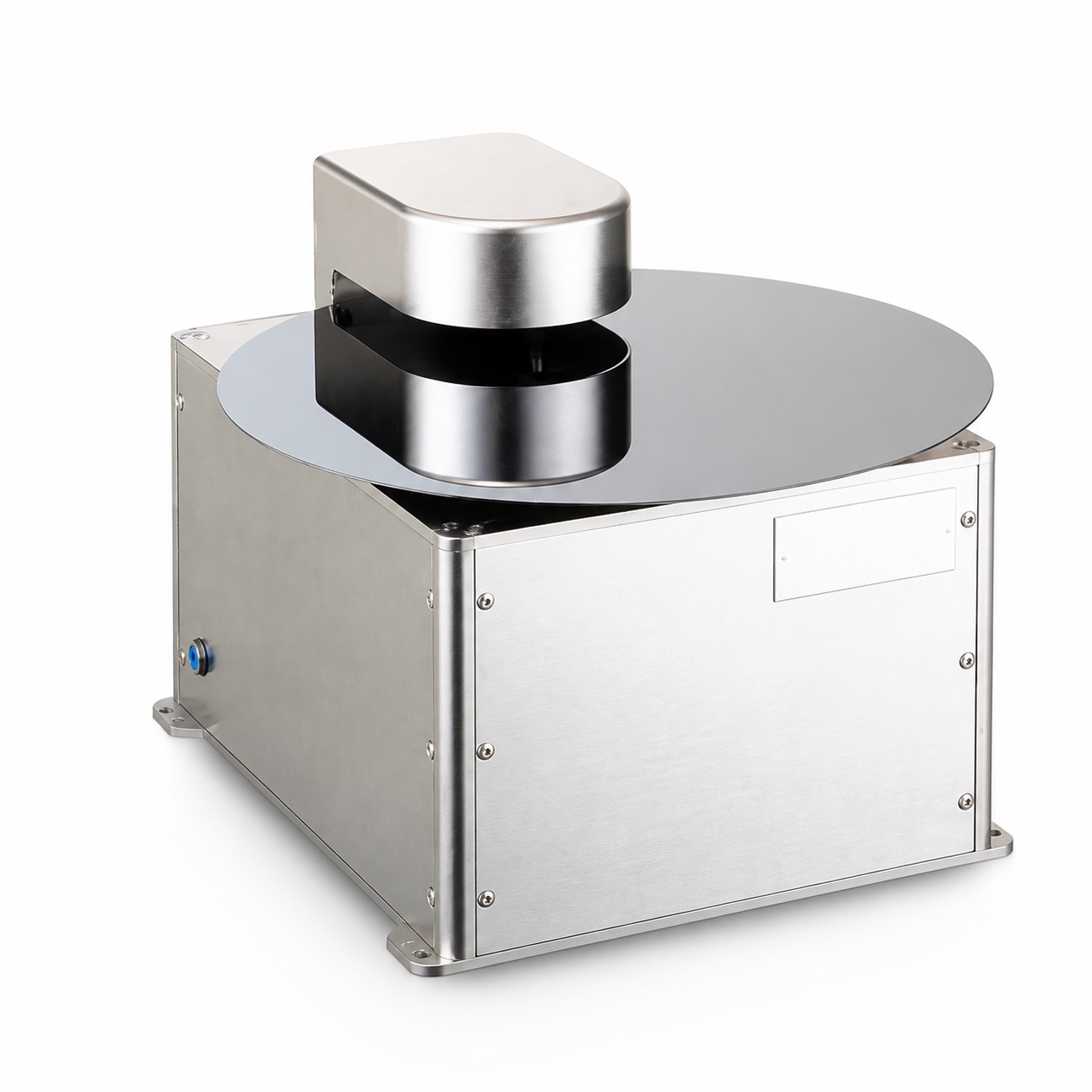
A wafer-image sensor and θ, X, and Z motion stages. A high-resolution linear CCD reads the edge and notch quickly, corrects eccentricity, and aligns the flat or notch to a user-set angle.
- Minimal-contact chuck to limit particles
- Inner filter for Class 1 and contamination control
- One unit handles 6", 8", and 12" wafers
- Footprint 248×285×230mm
- X, Z, and θ are modular for easier maintenance
- Cycle time under 4 seconds
- Micro-stepping drivers for precise positioning
- Precision X ±0.035mm / θ ±0.035mm
Drawings and additional documents are being prepared. If you need them, please technical inquiry. · ← Back to semiconductor equipment